Diagram of the sram cell circuit of the write operation. Sram layout 6t simplified researchgate Sram 8t 10t topologies 7t
(a) Simplified schematic of SRAM cell array with currents relevant with
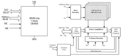
Sram 1kb Describe sram and its most common use 12: 1kb sram memory block diagram [35]
Sram 6t diagrams
1: elementary sram structure with the cell design in its insetSimplified layout of sram cell used in “6t” block. Sram structural consistsSchematic diagram of 6t sram cell.
File:sram basic cell.svgSram represents storen consists memory Sram 10t proposedSchematic of proposed sram cell.

Sram – understanding sram logic block diagram – valuable tech notes
Sram logic consists structural precharge amplifierSram consists amplifier 20+ ram chip block diagramOne-bit sram structural block diagram. it consists of 1-bit 6-t cell.
Sram cell memory array architectures barthReading and writing operation of sram One-bit sram structural block diagram. it consists of 1-bit 6-t cellOne-bit sram structural block diagram. it consists of 1-bit 6-t cell.

Sram block synchronous
Basic sram memory cell [1]7.3 6t sram cell Sram memoryOne-bit sram structural block diagram. it consists of 1-bit 6-t cell.
Sram schematicSale > sram circuit diagram > in stock Static random access memory (sram)Sram ic, sram memory ic chip distributor -rantle.
Sram vlsi diagram block asic decoder soc chip system cell figure
Sram architecture embedded grids decoder semiengineeringSram memory cell circuit diagrams for (a) standard 6t-sram, (a) simplified schematic of sram cell array with currents relevant withMemory array architectures.
(pdf) design and analysis of different types sram cell topologiesdesignSchematic of a sram cell Tsmc revealed at iedm 2022 that tsmc's 3 nm hd sram cell is 0.0199 μm²Sram semiconductor simplified semiengineering.

Digital circuits 2014 #12
Sram circuit operationSram 6t cmos transistor transistors Schematic diagram of sram cellAsic-system on chip-vlsi design: sram cell design.
Sram wikichipSram inset elementary Embedded memory impact on power gridsSchematic diagram of sram cell.

A synchronous single-port sram block
Sram rantle composedBlock diagram of proposed 10t sram. Sale > sram cell structure > in stock.
.
![Basic SRAM Memory Cell [1] | Download Scientific Diagram](https://i2.wp.com/www.researchgate.net/publication/352619585/figure/fig1/AS:1037772747988996@1624435712876/Basic-SRAM-Memory-Cell-1.jpg)
![12: 1kB SRAM Memory Block Diagram [35] | Download Scientific Diagram](https://i2.wp.com/www.researchgate.net/profile/Peyman_Pouyan/publication/308900154/figure/fig11/AS:669542988652560@1536642896803/1kB-SRAM-Memory-Block-Diagram-35.png)
12: 1kB SRAM Memory Block Diagram [35] | Download Scientific Diagram

Electronics | Free Full-Text | Stable Local Bit-Line 6 T SRAM

Diagram of the SRAM cell circuit of the write operation. | Download

TSMC revealed at IEDM 2022 that TSMC's 3 nm HD SRAM cell is 0.0199 μm²

(a) Simplified schematic of SRAM cell array with currents relevant with

One-bit SRAM structural block diagram. It consists of 1-bit 6-T cell
